Application PCB Designer or Layout software instal Use Very Easy
This time I will give a little tutorial on the application PCB Designer / pcb simulation / pcb circuit / program pcb as follows:[-] download the application PCB DESIGNER
[-] install the application PCB Designer.
[-] function the application PCB Designer
[-] uninstall the application PCB Designer
Before discussing some tutorial above I will give a little information and an overview of the application PCB Designer as follows:# Understanding the application PCB Designer
Application PCB Designer is an application that is used to create layouts on the circuit example (the series of twilight switches, dimers, AC Neon, etc.) pcb design and simulation software .Therefore this application is very important in the process of loading the circuit layout is nice and neat.# Menu on the application PCB Designer
- File- Edit
- Broad
- Text
- Snap
- Window
- Help
So that I can convey information about the application PCB Designer .directly course I will discuss about how to install the application PCB Designer as follows:
A. how to install the application PCB Designer
steps - steps as follows:1. Open the application setup on a PCB Designer.
2. Then you will be given the option to choose the language is English and french .(i suggest choosing English.)

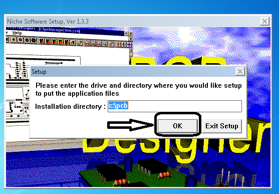
4. Wait for the installation process the application PCB Designer approximately takes about 10 seconds => and press YES.

READ TO Application EWB
B. Use of the application PCB Layout Designer
function application pcb designer is a
- layout
- circuit broad designer
- pcb program
- printer broad
- linux pcb
Steps - his steps as follows:
1. Open the application PCB Designer.
2. This time I will give an example of a string of a very simple and easy that a string layout Dimer.
FUNCTION Dimer is as a regulator circuit and the dimming of the light of his light on the light bulb.
3. List the name of the component as follows:
a. Lamp
b. TRIAC
c. DIAC
d. RESISTOR
e. NE
4. Draw a string layout Dimer switch.

if you are not clear / not familiar with the above tutorial .You can see VIDEOS about tutorial instal application PCB Designer as follows:
Steps instal application PCB Dsigner
the following:
1. Go to Start => contol panel.
2. Select the programs.

3. Select a program and features.

4. Locate and then click the application PCB several times on applications PCB Designer Until the screan like this.
5. Select YES.
6. Select OK.
7. If uinstal successfully as shown below.
thank you very much
C How to Uninstall Applications PCB Designer (Electronic Workbench)
Steps instal application PCB Dsigner
the following:
1. Go to Start => contol panel.
2. Select the programs.

3. Select a program and features.

4. Locate and then click the application PCB several times on applications PCB Designer Until the screan like this.
5. Select YES.
6. Select OK.
7. If uinstal successfully as shown below.
READ TO Application Proteus ISIS,ARES
Tutorial so that I can convey about the application PCB Designer, if you do not clear can ask in the comments.
Thank you very much for his visit.
Thank you very much for his visit.